1
Diode waveforms
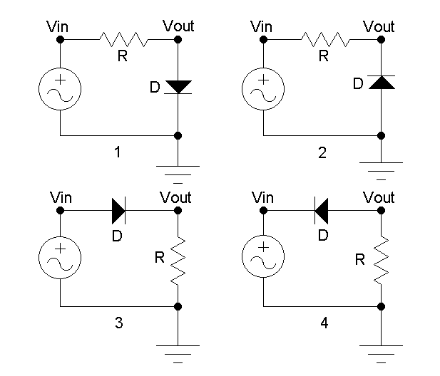
A basic diode circuit consists of a diode D in series with a current-limiting resistor R. There are four possible circuit configurations, as shown, depending on the location of the two components. A colored band on the diode and the bar on the diode symbol identify the negative or cathode side of the diode.To observe the circuit behaviour, remove any components used in the previous lab. For each of the four diode configurations:
- Connect the FG to the Vin node of the circuit and configure it to output a 1kHz sine wave of 8V amplitude and zero offset.
- Monitor Vin with the scope CH1. Monitor Vout with CH2.
- Match the CH1 and CH2 gains and align their V=0 positions on the screen.
- record a scope screenshot that clearly shows the relationship between Vin and Vout;
- determine the turn-on voltage Von for this Silicon diode;
- for both the positive and negative portions of the input sine wave, what is the voltage VR across R and VD across D?
- how are VR and VD related?
2
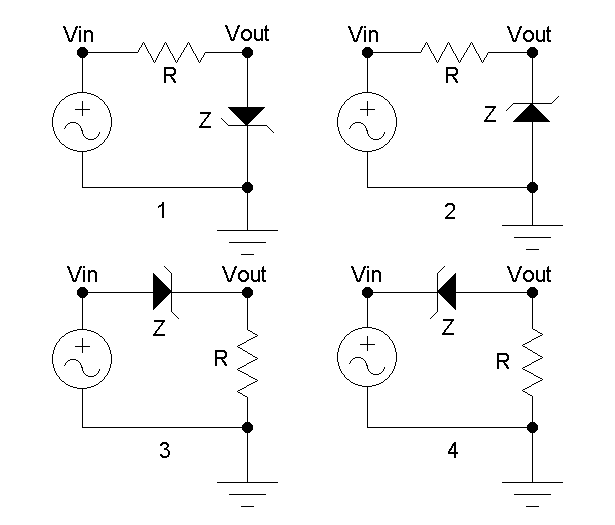
Zener diode waveforms
The Zener diode behaves as a regular diode when positively biased but will also begin to conduct when a negative bias voltage exceeds the Zener breakdown voltage VZ. To observe the Zener behaviour:- repeat the steps previously outlined for the diode;
- if Vout looks like a typical diode waveform, increase Vin until something unusual appears on the scope trace.
- determine VZ for this Zener diode.
- How does the Zener output waveform differ from that of the regular diode?
Note: Remove these components from your breadboard before proceeding to the next exercise.
1
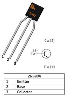
The 2N3904 transistor
To the left is a pinout and schematic symbol of the 2N3904 bipolar NPN silicon transistor. There are three connections; the emitter E, base B and collector C.The arrow between the base and the emitter represents a P-N junction, or diode . The voltage VBE across these two terminals determines whether a current will flow between the C-E terminals.
When a positive voltage VBE exceeds the turn-on voltage of the junction, the diode conducts current, otherwise, with lesser positive as well as negative voltages, it will not.
The turn-on voltage for a silicon P-N junction is around +0.7V,
In this region the current increases exponentially with an increase in voltage.
1
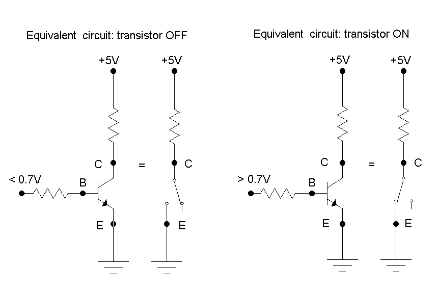
Transistor as a switch
When the voltage at the base pin exceeds by the voltage at the emitter pin by VBE > ≈ 0.7V, the diode conducts and- the collector-emitter junction resistance RCE ≈ 0Ω, hence the collector-emitter junction is effectively a short circuit,
- the collector-emitter junction voltage drop VCE ≈ 0V,
- the collector-emitter junction resistance RCE ≈ ∞, hence the collector-emitter junction is effectively an open circuit.
2
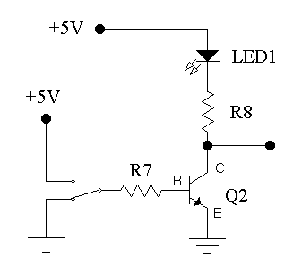
Transistor controls LED
The workstation comes with two three-position mechanical switches. With the rocker arm positioned at one end of the switch, the centre pin connects to the pin at the opposite end. With the rocker arm at centre, all pins are disconnected.- Starting with a flashing mystery circuit, disconnect R7 from pin.6 of IC2 and use a jumper to connect the open end of R7 to the centre pin of one of the switches.
- Use jumpers to connect one end of the switch to +5V and the other end to GND.
- Toggle the switch. The LED should go on and off.
- Set the switch so that +5V outputs at the centre pin, then use the multimeter to verify the voltage.
- Tabulate the switch voltage, the on/off state of the LED and the voltage at both ends of the LED, R7 and R8.
- Set the switch to output 0V and repeat the above steps.
3
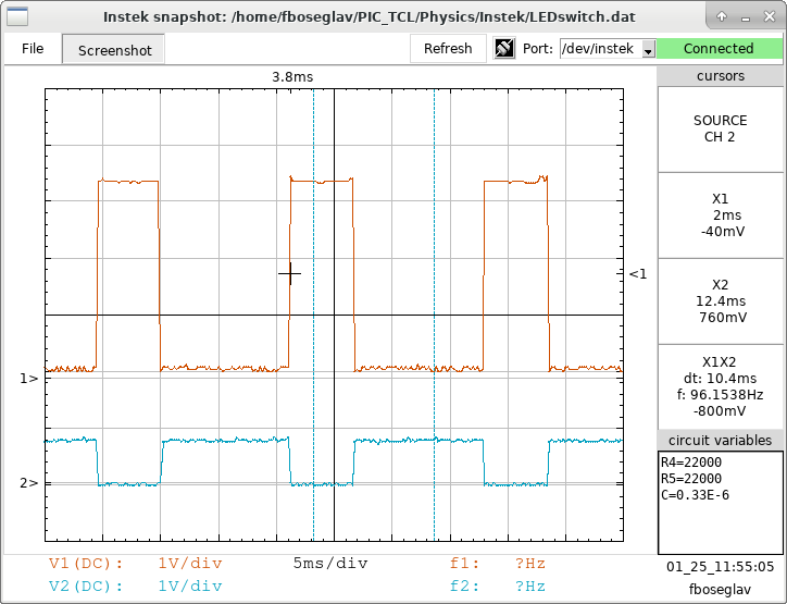
You can now repeat the previous measurements using the scope.
- Disconnect the switch from R7 and reconnect R7 to pin.6 of IC2 so that the mystery circuit operates as expected.
- Use a jumper to connect CH1 to the base of Q2.
- Use another jumper to connect CH2 to the collector of Q2.
- Press Autoset; two waveforms should appear as in the accompanying figure
- Select one of the waveforms in turn and use the cursors to measure and tabulate the high and low voltage levels VBE and VCE.
- Compare these results with those obtained previously when using the switch.
- Does this waveform represent VBE or VCE?
3
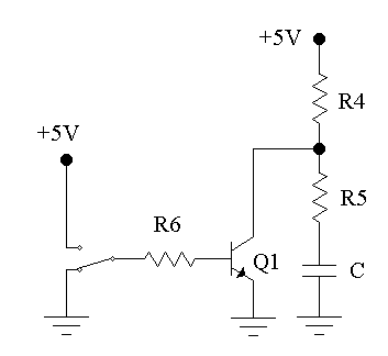
Transistor controls capacitor voltage
To better observe the interaction between transistor Q1 and the RC circuit, you can use a switch to manually control the transistor and thus the capacitor charge/discharge cycle. To setup the circuit:- use the original RC components: C = 10μF, R4 = R5 = 22kΩ,
- disconnect R7 from the switch and reconnect it to pin.6 of IC2,
- disconnect R6 from pin.5 of IC2 and connect it to the switch,
- connect Ch1 to the switch centre pin,
- connect Ch2 to the R5-C node.
4
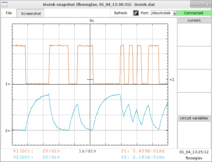
Transistor switched capacitor waveforms
- Toggle the switch and note how the capacitor voltage changes.
- Allow the transient voltage to settle, then use the cursors to carefully measure the voltage at each of the two limits of the charge/discharge cycle.
- Compare these voltage values to the power supply voltage, do you note a possible relationship?
- Quickly toggle the switch, what happens to the voltage at C? How might you relate this observation to the operation of the mystery circuit?
- Reproduce and save a trace similar to the one shown. How does the switch position affect the behaviour of the transistor and the charging/discharging of the capacitor?