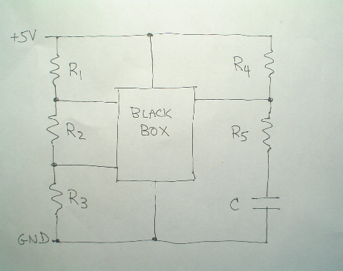
A block diagram of the mystery circuit
Sketches are a handy visual guide that allow you to integrate observations and focus on the components of interest. Make sketches similar to the ones shown, to facilitate the troubleshooting and analysis of your mystery circuit.The sketch on the left displays a basic schematic of the mystery circuit, grouped into functional blocks.
To the left is the resistor voltage divider ladder with connections to the black box.
To the right is the resistor/capacitor network that was previously analysed. It was determined that transistor Q1, here inside the black box, controls the state of the R4-R5 node and hence the charging and discharging of the capacitor.
Analysis of capacitor voltage
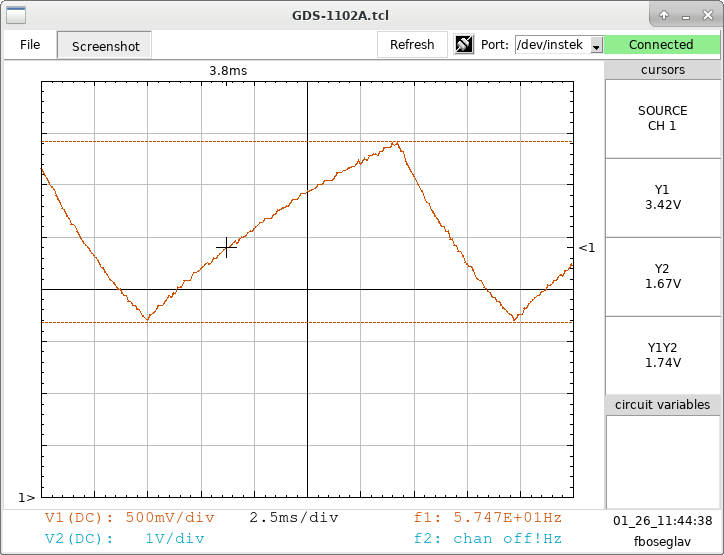
- Connect the scope Ch2 to the R5-C node to monitor the capacitor voltage.
- Use the multimeter to measure the power supply voltage.
- Measure and record the high VH and low VL limits of the capacitor voltage. What is the ratio of these two values relative to the power supply voltage?
- Measure and record the voltages at the R1-R2 and R2-R3 nodes of the voltage divider. What is the ratio of these values relative to the power supply voltage?
- What would these voltage ratios be in the ideal case where the values of R1, R2 and R3 are identical?
- Based on the above results, propose a possible functional relationship, realized within the black box, between the RC circuit and the resistor voltage divider.
Analytical derivation of the timing equation
Follow the steps outlined in the next slide to analytically determine the time delays tc and td between VH and VL for the capacitor charging and discharging cycles.
The timing equation is then T = tc + td. It should be algebraically equivalent to that previously derived using dimensional analysis.
Recall that the capacitor discharging from V0 to V1 is given by
and the capacitor charging from V0 to V1 is given by
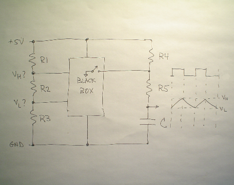
Square wave indicates switch state: high=open, low=closed
- use the discharging equation to solve for t = t1 at VH;
- use the discharging equation to solve for t = t2 at VL;
- evaluate td = t2 - t1 with R = Rd;
- use the charging equation to solve for t = t1 at VL;
- use the charging equation to solve for t = t2 at VH;
- evaluate tc = t2 - t1 with R = Rc;
- determine T = tc + td.
Repeat the above using your measured VH and VL results. Are the K1, k2 coefficients similar to those analytically derived?
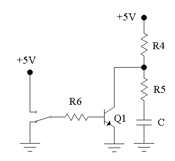
Manual control of capacitor charge/discharge
Instead of having the mystery circuit control the capacitor charge/discharge you can use a switch to control Q1 and hence the capacitor voltage. To set up the circuit:
- disconnect R6 from pin 5 of IC2
- connect R6 to the centre pin of a three-way switch;
- connect one end pin of the switch to 0V;
- connect the other end pini of the switch to 5V;
- use R4 = R5 = 22kΩ and C = 10μF.
- connect CH1 to the centre pin of the switch;
- connect CH2 to the R5-C node of the circuit;
- set the timebase to a 1s Roll.
Toggle the switch to vary the voltage at the capacitor. Try to reproduce the mystery circuit capacitor charge/discharge curve.
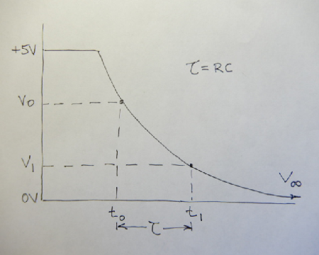
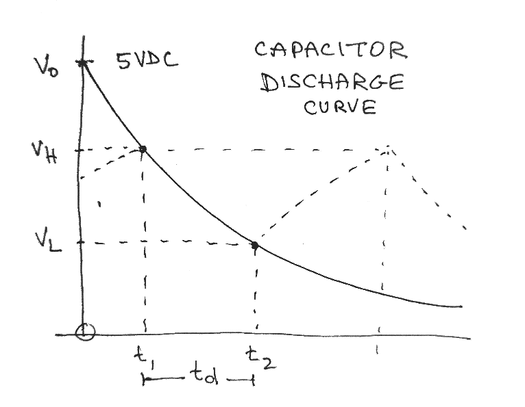
Measuring an RC constant
If the time between two points on a capacitor charge/discharge curve is such that t1 - t0 = τ = RC, then the charging/discharging equations can be generalized to
where V∞ is the voltage at the steady-state end of the transient. Displayed is a capacitor discharge curve. To measure τ:
- determine the correct value of V∞ to use;
- position one cursor at some voltage V0 along the transient;
- record the time t0 corresponding to V0;
- position the second cursor at the calculated voltage V1;
- record the time t1 corresponding to V1.
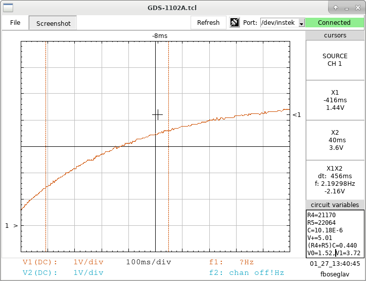
- calculate the theoretical τ for this circuit. Use the measured values for R4, R5, C and the +5V supply;
- toggle the switch to generate a full discharge curve;
- freeze the scope display and adjust the gain/timebase to zoom in on the exponential decay curve;
- follow the previously outlined steps;
- save a screenshot showing the cursors placement.
Try a couple of other initial V0 positions along the curve and compare these experimental results with the theoretical τ. Repeat for a capacitor charging curve, shown here.