1
The NAND gate
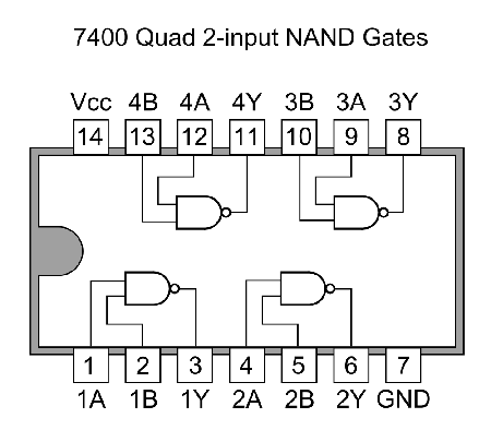
The The NAND (NOT-AND) gate is a logic unit that outputs a low voltage (logic 0) only when a high voltage (logic 1) is applied to all the inputs. Other logic functions such as NOT, OR, XOR can be implemented using NAND gates. Cross-coupling of NAND gates yields a digital memory cell known as a flip-flop.The 14-pin chip is now revealed as a device that incorporates four identical NAND logic gates. The way that the gates are connected will determine their function in the mystery circuit.
- Add to the 14-pin chip in your schematic diagram a sketch of the internal configuration of the logic gates, showing how each gate is connected to the rest of the circuit.
- Identify all the gate connections with pin numbers.
1
Logic synthesis using NAND gates
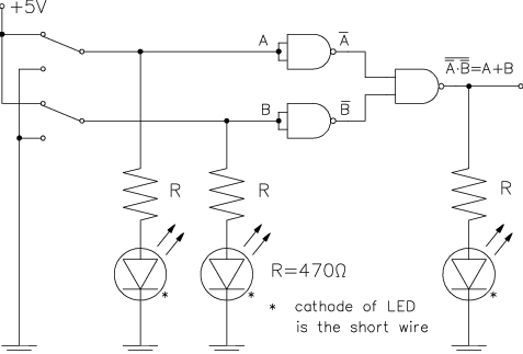
You will now explore how different logic elements can be constructed using various combinations of NAND gates. An OR gate is shown here. With the application of feedback, an RS or D flip-flop memory cell can be constructed.To avoid disassembling the mystery circuit, you will use another two 7400 chips since some circuits need more than four gates. Refer to these chips as IC3 and IC4.
- Extend the +5V and GND power rails to the second breadboard.
- Carefully insert IC3 and IC4 on the second breadboard.
- Make the +5V (pin.14) and GND (pin.7) connections to the chips.
- Use LEDs to monitor the gate inputs and outputs, as shown.
2
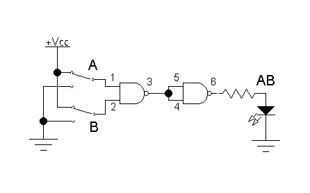
The circuit on the left uses a couple of NAND gates to implement the AND logic function.
Use the switches to set the input logic levels (VCC=5V='1', GND=0V='0'),
as previously described.
Observe the logic state of each switch and the output by using an LED in series with a 470Ω resistor (LEDon=1, LEDoff=0).
Observe the logic state of each switch and the output by using an LED in series with a 470Ω resistor (LEDon=1, LEDoff=0).
- Assemble the AND gate circuit as shown.
- Set the inputs A,B to VCC or GND and observe the output AB.
- Create a truth table of all the possible input combinations.
- What logic operation does the second gate perform?
- Label all gate outputs with their Boolean function. For the AND circuit, pin.3 is (AB)' and pin.6 is (AB)'' or AB.
- an OR gate with output A+B;
- an XOR gate with output A XOR B;
- a half-adder with outputs S (sum) and C (carry). Add a second LED to monitor both outputs.
What is the logic equivalent of the half-adder S output?
What is the logic equivalent of the half-adder C output?
3
Digital memory cell using NAND gates
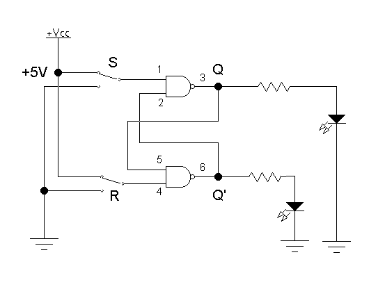
Shown is a pair of cross-coupled NAND gates called an SR (Set-Reset) flip-flop. There are two complementary outputs, called Q and Q'. One input, called R, resets Q, i.e. sets Q=0. The other input, called S, sets Q=1.- Assemble the circuit shown and analyse the logic operation as before.
- Carefully document how the Q and Q' outputs change as you toggle an R or S input between levels 0<->1, while keeping the other input constant.
- What combinations of input states lead to logically inconsistent, or 'illegal' output states?
- Determine the additional logic required to implement a D-flip-flop then build the circuit and redo the analysis to show that the 'illegal' condition has been eliminated.
3
A summary of the mystery circuit
You now have a complete schematic of the mystery circuit. It can be seen that the circuit operation involves a feedback loop where the voltage at the capacitor controls the outputs of the comparators which serve as inputs to the 7400 logic which in turn provides an output that controls the on/off state of the transistor that in turn controls the charge/discharge of the capacitor.- What logic function is your mystery circuit 14-pin chip IC2 wired to perform? What constraint does this circuit place on the output states of the two comparators connected to it?
- the two IC1 outputs at pins 1 and 7, call these C1 and C7;
- the IC2 flip/flop input pins R, S and output pins Q, Q';
- the base voltage Vb and collector voltage Vc of Q1.
1
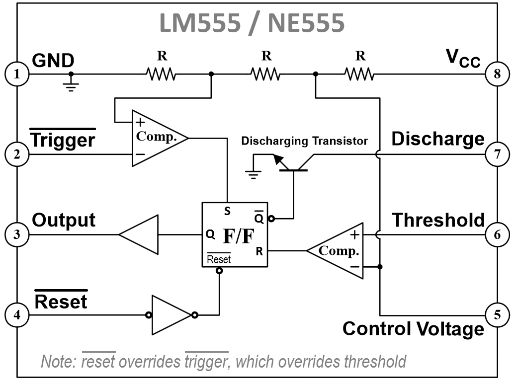
The 555 timer
It turns out that there is a chip available, the popular 555 timer integrated circuit (IC) that incorporates all of the functionality of your mystery circuit. There are several advantages to integrating these components onto a single integrated circuit:- the mystery circuit is reduced to the size of an 8-pin chip;
- the circuit is much more reliable and less prone to interference from noise and stray capacitances and resistances since most of the connections are internal to the chip;
- an integrated circuit is able to operate much faster since most of these internal connections between components are much shorter, in the order of micrometers (um).
The 555 data sheet can be found here. The 555 pinout and internal schematic the are shown in the accompanying figure.
2
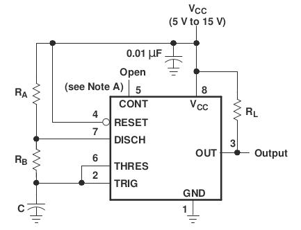
Astable operation
The 555 timer can perform a variety of timing functions. The timing, as you have discovered for the mystery circuit, is determined by the three external components, C, R4 and R5. These are also the only external components required to control the timing of the 555 timer.Your mystery circuit was configured as an astable oscillator, as is the 555 timer shown in the figure. It outputs pulses of period
- Compare your completed schematic diagram of the mystery circuit with that of the figure. Note any differences.
- Label on your circuit schematic the connections (nodes) of the mystery circuit that correspond to the pins of the 555 timer.
- Note any differences between the mystery circuit and the 555 timer chip.